| CPC H01L 21/823814 (2013.01) [H01L 21/02532 (2013.01); H01L 21/02576 (2013.01); H01L 21/02579 (2013.01); H01L 21/0259 (2013.01); H01L 21/823807 (2013.01); H01L 21/823871 (2013.01); H01L 27/092 (2013.01); H01L 29/0665 (2013.01); H01L 29/41733 (2013.01); H01L 29/42392 (2013.01); H01L 29/7845 (2013.01); H01L 29/78618 (2013.01); H01L 29/78696 (2013.01)] | 14 Claims |
|
1. A semiconductor structure, comprising:
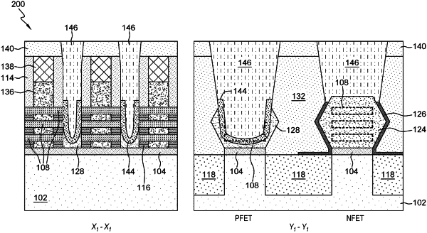
a first nanosheet field-effect transistor formed on a first portion of a substrate, the first nanosheet field-effect transistor formed on the first portion of the substrate includes a first source drain epitaxy, wherein a top surface of the first source drain epitaxy is above a top surface of a top-most nanosheet channel layer;
a second nanosheet field-effect transistor formed on a second portion of the substrate, the second nanosheet field-effect transistor formed on the second portion of the substrate includes a second source drain epitaxy and a third source drain epitaxy, wherein the second source drain epitaxy is below the third source drain epitaxy, wherein the third source drain epitaxy is u-shaped and is directly connected to at least one nanosheet channel layer; and
one or more metal contacts, wherein at least one of the one or more metal contacts extends vertically from a top surface of an interlayer dielectric to the at least one nanosheet channel layer.
|