| CPC H01L 21/823481 (2013.01) [H01L 21/76224 (2013.01); H01L 21/823431 (2013.01); H01L 27/0886 (2013.01); H01L 29/0649 (2013.01); H01L 21/31053 (2013.01)] | 20 Claims |
|
1. A semiconductor device structure, comprising:
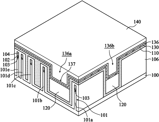
a first fin, a second fin and a third fin between the first fin and the second fin that protrude from a substrate, wherein the third fin is spaced apart from the first fin by a first width and spaced apart from the second fin by a second width less than the first width;
a first insulating structure formed over the substrate, comprising:
a first insulating layer formed between the first fin and the third fin;
a capping structure covering a top surface of the first insulating layer;
a first insulating liner covering sidewall surfaces of the first insulating layer and the capping structure and a bottom surface of the first insulating layer; and
a second insulating liner formed between the first insulating liner and the first fin and between the first insulating liner and the third fin; and
a second insulating structure formed over the substrate, comprising:
a second insulating layer formed between the second fin and the third fin; and
a third insulating liner formed between the second insulating layer and the second fin and between the second insulating layer and the third fin.
|