| CPC H01L 21/823475 (2013.01) [H01L 21/76802 (2013.01); H01L 21/76877 (2013.01); H01L 23/5226 (2013.01); H01L 29/401 (2013.01); H01L 29/42392 (2013.01); H01L 29/78696 (2013.01)] | 20 Claims |
|
1. A method, comprising:
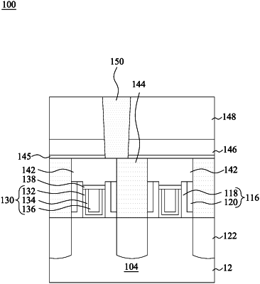
forming a gate structure over a semiconductor substrate;
forming a gate dielectric cap over the gate structure;
forming source/drain contacts over the semiconductor substrate, with the gate dielectric cap between the source/drain contacts;
depositing an etch-resistant layer over the gate dielectric cap;
depositing a contact etch stop layer over the etch-resistant layer and an interlayer dielectric (ILD) layer over the contact etch stop layer;
performing a first etching process to form a via opening extending through the ILD layer and terminating prior to reaching the etch-resistant layer;
performing a second etching process to deepen the via opening such that one of the source/drain contacts is exposed, wherein the second etching process etches the etch-resistant layer at a slower etch rate than etching the contact etch stop layer, wherein the second etching process stops when a bottom of the via opening reaches a top surface of the gate dielectric cap; and
depositing a metal material to fill the deepened via opening.
|