| CPC H01L 21/823412 (2013.01) [H01L 21/02274 (2013.01); H01L 21/0228 (2013.01); H01L 21/02565 (2013.01); H01L 29/66969 (2013.01); H01L 29/786 (2013.01); H01L 29/78696 (2013.01); H01L 29/66742 (2013.01)] | 13 Claims |
|
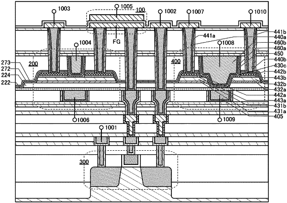
1. A manufacturing method of a semiconductor device comprising a first conductor, first and second insulators, and first to third oxides, comprising the steps of:
forming the first oxide over a substrate;
forming a second oxide over the first oxide;
depositing the first insulator over the first oxide;
forming an opening reaching the first oxide in the first insulator and the second oxide;
depositing a first oxide film in contact with the first oxide and the first insulator in the opening;
depositing a first insulating film over the first oxide film by a PEALD method;
depositing a first conductive film over the first insulating film; and
removing part of the first oxide film, part of the first insulating film, and part of the first conductive film until a top surface of the first insulator is exposed to form the third oxide, the second insulator, and the first conductor,
wherein the second oxide does not overlap with the third oxide, the second insulator, and the first conductor,
wherein the first oxide, the first oxide film, and the first insulator are irradiated with a microwave before the first insulating film is deposited.
|