| CPC H01L 21/78 (2013.01) [H01L 21/306 (2013.01); H01L 21/56 (2013.01); H01L 21/561 (2013.01); H01L 23/3114 (2013.01); H01L 23/482 (2013.01); H01L 29/0657 (2013.01)] | 15 Claims |
|
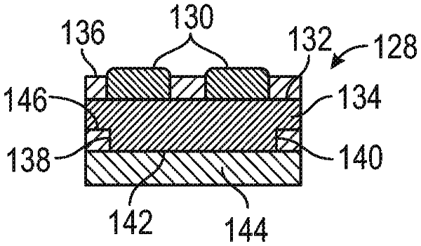
1. A semiconductor package comprising:
a die comprising a notch located around a perimeter of a sixth side of the die, the die comprising a first side opposing the sixth side, the first side of the die comprising a plurality of electrical contacts;
a second molding compound coupled over the sixth side of the die and into the notch;
a first molding compound coupled over the first side of the die, the first molding compound forming a thickness above the first side; and
a metal layer coupled to the sixth side of the die;
wherein a thickness of the plurality of electrical contacts is substantially the same as the thickness of the first molding compound;
wherein an entirety of the second molding compound is coupled between the metal layer and the die;
wherein each of the metal layer, the second molding compound, and the die all extend to an outermost side surface of the semiconductor package.
|