| CPC H01L 21/76898 (2013.01) [H01L 23/481 (2013.01)] | 11 Claims |
|
1. A method comprising:
providing a semiconductor substrate having a semiconductor device disposed over the semiconductor substrate;
depositing a first dielectric layer over the semiconductor device;
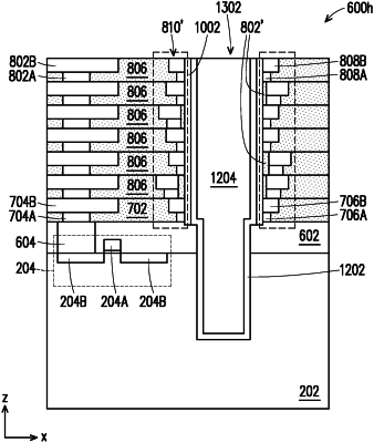
forming, within the first dielectric layer, a first via, a first metal line over the first via, a first metal ring coplanar with the first via, and a second metal ring coplanar with the first metal line and on the first metal ring;
depositing a second dielectric layer over the first metal line;
forming, within the second dielectric layer, a second via, a second metal line over the second via, a third metal ring coplanar with the second via and on the second metal ring, and a fourth metal ring coplanar with the second metal line and on the third metal ring; and
forming another via through a portion of the semiconductor substrate, wherein the forming the another via includes etching the first dielectric layer and the second dielectric layer to form an opening extending through a center region of each of the first metal ring, the second metal ring, the third metal ring, and the fourth metal ring, wherein at least one of the first metal ring, the second metal ring, the third metal ring, and the fourth metal ring are laterally etched during the etching to form the opening.
|