| CPC H01L 21/7685 (2013.01) [C23C 16/34 (2013.01); C23C 16/345 (2013.01); C23C 16/42 (2013.01); C23C 16/45527 (2013.01); C23C 16/45529 (2013.01); C23C 28/00 (2013.01); C23C 28/321 (2013.01); C23C 28/34 (2013.01); C23C 28/345 (2013.01); C23C 28/36 (2013.01); H01L 21/02068 (2013.01); H01L 21/28518 (2013.01); H01L 21/28562 (2013.01); H01L 21/76841 (2013.01); H01L 23/53266 (2013.01); H01L 21/76846 (2013.01)] | 30 Claims |
|
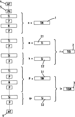
1. A method of forming an electrically conductive diffusion barrier, the method comprising:
providing a substrate comprising an exposed silicon surface formed of monocrystalline silicon or polycrystalline silicon in a reaction chamber;
forming a titanium silicide (TiSi) region of the diffusion barrier directly on the exposed silicon surface of the substrate by alternatingly exposing the substrate to a first titanium-containing precursor and a first silicon-containing precursor; and
forming a titanium silicon nitride (TiSiN) region of the diffusion barrier directly on the TiSi region by alternatingly exposing the substrate to a second titanium-containing precursor, a nitrogen-containing precursor and a second silicon-containing precursor,
wherein the TiSi region and the TiSiN region are formed in situ, and
wherein a combined thickness of the TiSi region and the TiSiN region does not exceed 10 nm.
|