| CPC H01L 21/76831 (2013.01) [H01L 21/30608 (2013.01); H01L 21/30655 (2013.01); H01L 21/823412 (2013.01); H01L 21/823431 (2013.01); H01L 27/0886 (2013.01); H01L 21/02236 (2013.01); H01L 21/02247 (2013.01); H01L 21/02381 (2013.01); H01L 21/0243 (2013.01); H01L 21/0245 (2013.01); H01L 21/02488 (2013.01); H01L 21/02507 (2013.01); H01L 21/02532 (2013.01); H01L 21/3065 (2013.01)] | 20 Claims |
|
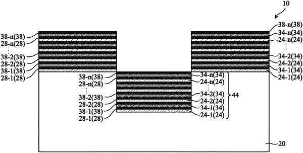
1. A method comprising:
depositing a first semiconductor layer, wherein the first semiconductor layer comprises:
a first bottom portion at a bottom of a trench in a semiconductor substrate; and
a first sidewall portion on a sidewall of the semiconductor substrate, with the sidewall of the semiconductor substrate facing the trench;
passivating the first semiconductor layer to form a first dielectric layer on a first remaining portion of the first semiconductor layer;
depositing a second semiconductor layer over the first dielectric layer, wherein the first semiconductor layer and the second semiconductor layer are formed of different semiconductor materials; and
passivating the second semiconductor layer to form a second dielectric layer over a second remaining portion of the second semiconductor layer.
|