US 11,942,362 B2
Surface modification layer for conductive feature formation
Jian-Jou Lian, Tainan (TW); Kuo-Bin Huang, Jhubei (TW); Neng-Jye Yang, Hsinchu (TW); and Li-Min Chen, Zhubei (TW)
Assigned to Taiwan Semiconductor Manufacturing Company, Ltd., Hsinchu (TW)
Filed by Taiwan Semiconductor Manufacturing Co., Ltd., Hsinchu (TW)
Filed on Mar. 6, 2023, as Appl. No. 18/178,948.
Application 18/178,948 is a continuation of application No. 16/914,788, filed on Jun. 29, 2020, granted, now 11,600,521.
Application 16/914,788 is a continuation of application No. 16/145,457, filed on Sep. 28, 2018, granted, now 10,699,944, issued on Jun. 30, 2020.
Prior Publication US 2023/0207384 A1, Jun. 29, 2023
This patent is subject to a terminal disclaimer.
Int. Cl. H01L 21/00 (2006.01); H01L 21/02 (2006.01); H01L 21/306 (2006.01); H01L 21/48 (2006.01); H01L 21/768 (2006.01); H01L 23/522 (2006.01); H01L 23/532 (2006.01)
CPC H01L 21/76823 (2013.01) [H01L 21/02307 (2013.01); H01L 21/30604 (2013.01); H01L 21/4857 (2013.01); H01L 21/76814 (2013.01); H01L 21/76826 (2013.01); H01L 21/76831 (2013.01); H01L 23/5226 (2013.01); H01L 23/5329 (2013.01)] 20 Claims
OG exemplary drawing
 
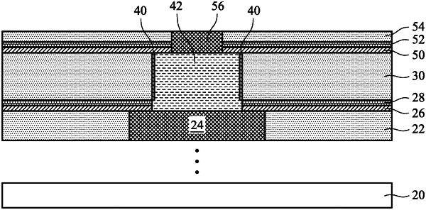
1. A semiconductor device comprising:
a dielectric layer over a conductive region over a semiconductor substrate;
an opening through the dielectric layer and exposing the conductive region;
a monolayer of material lining the opening adjacent to the dielectric layer, the monolayer of material comprising a phosphoric acid derivative material; and
conductive material within the opening.