| CPC H01L 21/7682 (2013.01) [H01L 21/0226 (2013.01); H01L 21/764 (2013.01)] | 15 Claims |
|
1. A method, comprising:
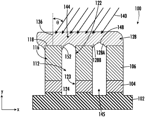
providing a plurality of semiconductor structures and a plurality of trenches of a semiconductor device;
forming a dielectric atop the plurality of semiconductor structures by:
delivering a dielectric material at a non-zero angle of inclination relative to a normal extending perpendicular from a top surface of the plurality of semiconductor structures; and
delivering the dielectric material at a second non-zero angle of inclination relative to the normal extending perpendicular from the top surface of the plurality of semiconductor structures, wherein the dielectric material forms a dielectric bridge extending over a cavity within at least one trench of the plurality of trenches.
|