| CPC H01L 21/76243 (2013.01) [C30B 15/206 (2013.01); C30B 29/06 (2013.01); H01L 21/3226 (2013.01); H01L 21/76251 (2013.01); H01L 23/66 (2013.01); H01L 27/1203 (2013.01); H01L 29/0649 (2013.01); H01L 2223/6661 (2013.01)] | 31 Claims |
|
1. A method of preparing a multilayer structure, the method comprising:
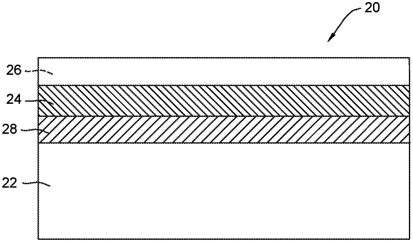
providing a single crystal semiconductor handle substrate comprising two major, generally parallel surfaces, one of which is a front surface of the single crystal semiconductor handle substrate and the other of which is a back surface of the single crystal semiconductor handle substrate, a circumferential edge joining the front and back surfaces of the single crystal semiconductor handle substrate, and a central plane of the single crystal semiconductor handle substrate between the front and back surfaces of the single crystal semiconductor handle substrate, wherein the single crystal semiconductor handle substrate has a bulk resistivity of at least about 5000 ohm-cm, an interstitial oxygen concentration of less than about 1×10¹⁶ atoms/cm3, a nitrogen concentration of at least about 1×10¹³ atoms/cm3, and an excess thermal donor concentration of less than 1×10¹¹ donors/cm3;
depositing a trap rich layer on the front surface of the single crystal semiconductor handle substrate;
bonding a front surface of a single crystal semiconductor donor substrate to the trap rich layer to thereby form a bonded structure, wherein the single crystal semiconductor donor substrate comprises two major, generally parallel surfaces, one of which is the front surface of the semiconductor donor substrate and the other of which is a back surface of the semiconductor donor substrate, a circumferential edge joining the front and back surfaces of the semiconductor donor substrate, and a central plane between the front and back surfaces of the semiconductor donor substrate; and
annealing the bonded structure.
|