| CPC H01L 21/76224 (2013.01) [H01L 21/76202 (2013.01); H01L 27/0203 (2013.01); H01L 29/0649 (2013.01)] | 17 Claims |
|
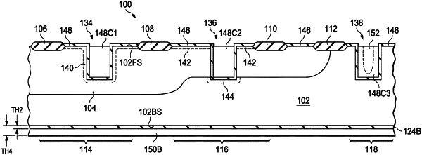
1. A method of forming an integrated circuit, comprising:
concurrently forming a first front end of line (FEOL) layer at a frontside of a semiconductor substrate and a second FEOL layer at a backside of the semiconductor substrate opposite the frontside, wherein the first and second FEOL layers include a same material, and wherein the second FEOL layer has a first thickness; and
removing at least a portion of the second FEOL layer such that the second FEOL layer has a second thickness less than the first thickness as a result of removing at least the portion of the second FEOL layer.
|