| CPC H01L 21/76224 (2013.01) [H01L 21/31116 (2013.01); H01L 21/823481 (2013.01)] | 20 Claims |
|
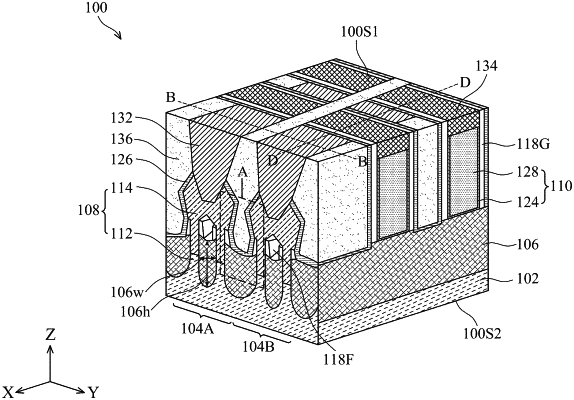
1. A method, comprising:
forming, on a substrate, first and second stacks of semiconductor layers with an opening in between, wherein the first and second stacks of semiconductor layers comprise first and second semiconductor layers stacked in an alternating configuration;
depositing a flowable isolation material in the opening;
densifying the deposited flowable isolation material with a plasma of oxygen radicals and hydrogen radicals; and
removing a portion of the densified flowable isolation material between the first and second stacks of semiconductor layers, wherein a top surface of the densified flowable isolation material is below bottom layers of the first and second stacks of semiconductor layers.
|