| CPC H01L 21/6836 (2013.01) [B32B 27/08 (2013.01); B32B 27/308 (2013.01); B32B 27/36 (2013.01); C09J 7/29 (2018.01); C09J 7/385 (2018.01); H01L 21/78 (2013.01); B32B 2405/00 (2013.01); C09J 2433/006 (2013.01); C09J 2467/006 (2013.01); C09J 2475/006 (2013.01)] | 5 Claims |
|
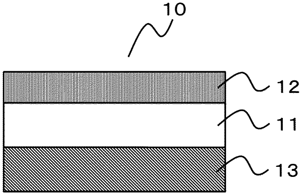
1. A semiconductor processing adhesive tape, comprising:
a base, a buffer layer provided at least on one surface of the base, and an adhesive layer provided on another surface of the base, wherein:
a Young's modulus at 23° C. of the buffer layer is 10 to 63 MPa and a breaking energy at 23° C. of the buffer layer is 1 to 9 MJ/m3, and
a Young's modulus at 23° C. of the base is larger than the Young's modulus at 23° C. of the buffer layer.
|