| CPC H01L 21/6835 (2013.01) [H01L 25/0753 (2013.01); H01L 33/62 (2013.01); H01L 2221/68354 (2013.01); H01L 2221/68363 (2013.01); H01L 2933/0066 (2013.01)] | 12 Claims |
|
1. A method for manufacturing an LED display, comprising:
picking up a plurality of LED chips spaced apart at a first interval with a stretchable stamp;
spacing apart the plurality of LED chips at a second interval by stretching the stretchable stamp; and
transferring the plurality of LED chips to a target substrate,
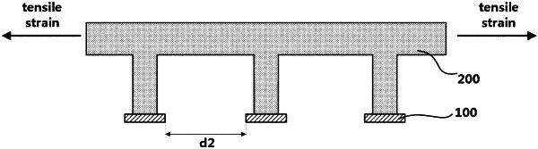
using a plurality of pick-up pillars comprising a cylinder portion connected to the body and a top portion having a larger cross-sectional area than the cylinder portion on the upper surface of the cylinder portion,
wherein the cross-sectional area ratio of the cylinder portion and the top portion is 100:130 to 100:300, and
wherein the cylinder portion and the top portion each have a columnar shape.
|