| CPC H01L 21/683 (2013.01) [C09J 7/20 (2018.01); C09J 7/22 (2018.01); C09J 201/00 (2013.01); H01L 21/67092 (2013.01); H01L 21/67098 (2013.01); H01L 21/67721 (2013.01); H01L 21/6836 (2013.01); B32B 43/006 (2013.01); C09J 2203/326 (2013.01); G01R 1/0491 (2013.01); G01R 31/2831 (2013.01); H01L 21/0201 (2013.01)] | 8 Claims |
|
1. A method for manufacturing a semiconductor component comprising:
a bonding step of bonding an adhesive layer of a film for manufacturing semiconductor components to a second surface of a semiconductor wafer having circuits formed on a first surface, the film comprising the adhesive layer formed of an energy-non-curing adhesive which is not cured by energy rays and a base layer provided on one surface side of the adhesive layer, and the ratio REI E(100)/E(25)) of the elastic modulus F(100) of the base layer at 100° C. to the elastic modulus E(25) of the base layer at 25° C. is such that 0.2≤RE1≤1, and the elastic modulus E′(25) is 35 MPa or more and 3500 MPa or less,
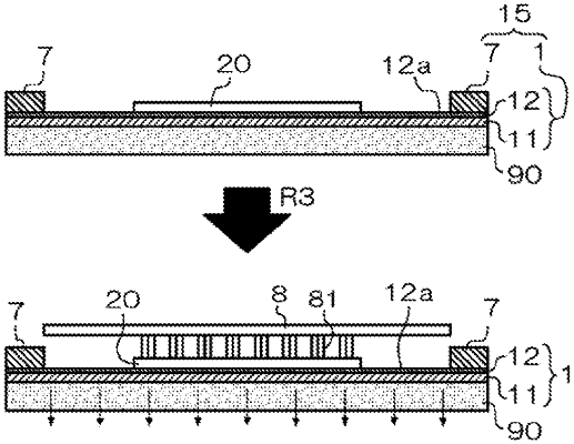
a segmenting step of separating the semiconductor wafer into segments in a state in which the adhesive layer of the film is bonded to the second surface of the semiconductor wafer,
an evaluation step of evaluating the semiconductor wafer or the semiconductor components at a temperature of 75° C. or higher, and
a pickup step of separating the semiconductor components from the adhesive layer,
wherein an arithmetic average roughness (Ra) of the surface of one side of the base layer on which the adhesive layer is not provided is 0.1 μm or more and 2.0 μm or less, and a maximum height (Rz) is 1.0 μm or more and 15 μm or less,
wherein the evaluation step further comprises:
either before or after the segmenting step and prior to the pickup step, a film-suction step of suctioning and fixing the base layer to a suction table, and
a film-isolating step of separating the suction table and the film from each other before a temperature of the suction table becomes room temperature after the evaluation step.
|