| CPC H01L 21/67259 (2013.01) [B25J 11/0095 (2013.01); G05B 19/00 (2013.01); G05B 2219/00 (2013.01); H01L 21/68707 (2013.01)] | 20 Claims |

|
18. A semiconductor processing tool, comprising:
a chamber;
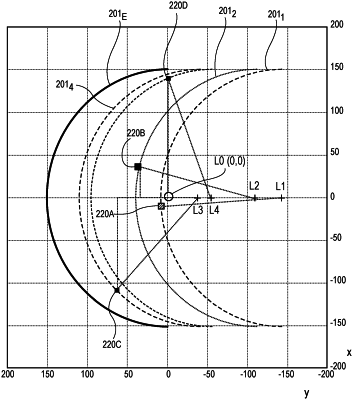
a plurality of pyrometers arranged about a bottom or top surface of the chamber;
a plurality of lamps opposite from the plurality of pyrometers;
a robot arm for inserting substrates into the chamber, wherein the robot arm is displaceable in a first direction and a second direction orthogonal to the first direction; and
a processor, wherein the processor includes instructions for centering substrates in the chamber using readings from the plurality of pyrometers, wherein centering substrates in the chamber is done without opening the chamber.
|