| CPC H01L 21/324 (2013.01) [C23C 16/4405 (2013.01); C23C 16/46 (2013.01)] | 20 Claims |
|
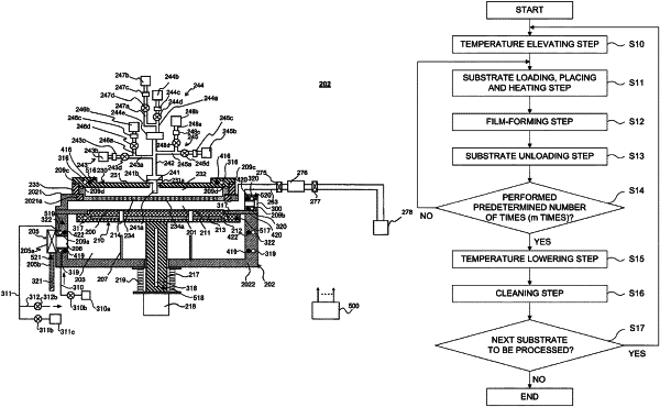
1. A method of manufacturing a semiconductor device, comprising:
(a) heating a substrate to a first temperature while supplying a process gas into a process vessel accommodating a substrate support;
(b) lowering a temperature of a low temperature structure provided in the process vessel to a second temperature lower than the first temperature by supplying a coolant to a coolant flow path provided in the process vessel for a predetermined time after (a), wherein a defect occurs when a cleaning gas is supplied to the low temperature structure at the first temperature; and
(c) cleaning the low temperature structure by supplying the cleaning gas into the process vessel after (b),
wherein the low temperature structure comprises at least one selected from the group consisting of:
a material provided with a coating capable of preventing corrosion due to the process gas is applied;
a structure located in vicinity of a viewport where through an inside of the process vessel is visually recognizable from an outside of the process vessel; and
a seal provided around the coolant flow path.
|