| CPC H01L 21/31144 (2013.01) [H01L 21/31116 (2013.01)] | 14 Claims |
|
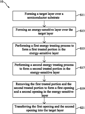
1. A method for preparing a semiconductor device structure, comprising:
forming a target layer over a semiconductor substrate;
forming an energy-sensitive layer over the target layer;
performing a first energy treating process to form a plurality of first treated portions in the energy-sensitive layer;
performing a second energy treating process to form a plurality of second treated portions in the energy-sensitive layer;
removing the first treated portions and the second treated portions to respectively form a plurality of first openings and a plurality of second openings;
transferring the first openings and the second openings into the target layer to respectively form a plurality of third openings and a plurality of fourth openings;
transferring the third openings and the fourth openings into the semiconductor substrate to respectively form a plurality of fifth openings and a plurality of sixth openings; and
filling the fifth openings and the sixth openings with an isolation structure;
wherein the first treated portions extend along a first direction, and the second treated portions extend along a second direction different from the first direction;
wherein the first treated portions are parallel to each other, and wherein each of the second treated portions is located between and in direct contact with any two adjacent ones of the first treated portions.
|