| CPC H01L 21/31051 (2013.01) | 20 Claims |
|
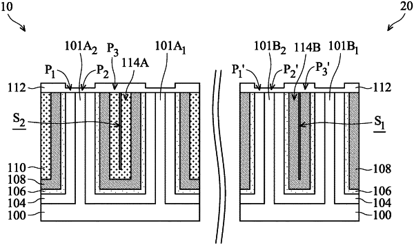
1. A method for forming a semiconductor device structure, comprising:
forming a semiconductor protruding structure over a substrate;
forming an insulating layer along sidewalls and a top of the semiconductor protruding structure;
forming a dielectric layer over the insulating layer;
planarizing the dielectric layer and the insulating layer to expose the top of the semiconductor protruding structure, wherein a remaining portion of the dielectric layer forms a dielectric structure;
forming a protective element to cover a top of the dielectric structure; and
recessing the insulating layer after the protective element is formed such that the semiconductor protruding structure and the dielectric structure protrude from a top surface of a remaining portion of the insulating layer.
|