| CPC H01L 21/3043 (2013.01) [H01L 29/1602 (2013.01); H01L 29/1608 (2013.01)] | 20 Claims |

|
1. A system, comprising:
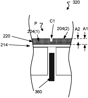
a wafer chuck, the wafer chuck being configured to receive a silicon carbide (SiC) semiconductor wafer thinned to a first thickness to produce a thinned SiC semiconductor wafer, a first surface of the thinned SiC semiconductor wafer being aligned along a plane;
a dicing apparatus configured to perform a partial dicing operation on the first surface of the thinned SiC semiconductor wafer to define a cut within the thinned SiC semiconductor wafer to produce a partially diced SiC semiconductor wafer, the cut having a depth less than the first thickness of the thinned SiC semiconductor wafer, the cut being aligned along a vertical direction orthogonal to the plane, the cut being aligned such that a portion of the thinned SiC semiconductor wafer has a second thickness that extends between a bottom of the cut and a second surface of the thinned SiC semiconductor wafer, the second surface being opposite the first surface; and
a cleaving apparatus, the cleaving apparatus being configured to perform a cleaving operation on the second surface of the partially diced SiC semiconductor wafer, through the portion of the partially diced SiC semiconductor wafer having the second thickness, along the vertical direction to define a cleave, the cleave being aligned with the cut and extending to the second surface of the partially diced SiC semiconductor wafer.
|