| CPC H01L 21/28581 (2013.01) [H01L 21/0217 (2013.01); H01L 21/3215 (2013.01); H01L 29/1066 (2013.01); H01L 29/2003 (2013.01); H01L 29/205 (2013.01); H01L 29/47 (2013.01); H01L 29/66462 (2013.01); H01L 29/7786 (2013.01)] | 20 Claims |
|
1. A process of forming an electronic device comprising:
forming a barrier layer;
forming a gate electrode layer over the barrier layer, wherein forming the gate electrode layer comprises:
forming a first film of the gate electrode layer, wherein the first film includes a first III-V material;
forming a first dopant region of the gate electrode layer, wherein the first dopant region has a first conductivity type;
forming a second film of the gate electrode layer overlying the first film of the gate electrode layer, wherein the second film includes a second III-V material and is formed after forming the first dopant region; and
forming a second dopant region of the gate electrode layer, wherein the second dopant region overlies the first dopant region and has the first conductivity type;
merging the first dopant region and the second dopant region together to form a diffused doped region by diffusing a dopant from each of the first dopant region and the second dopant region;
patterning the gate electrode layer to form a gate electrode; and
forming a gate interconnect over the gate electrode,
wherein after forming the gate interconnect, a first portion of the gate electrode contacts the barrier layer and is undoped or has an average dopant concentration of the first conductivity type that is at most 5×10¹⁶ atoms/cm3.
|
|
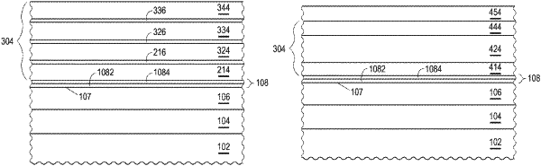
12. The process of claim 1, forming the barrier layer comprises:
forming a first film of the barrier layer; and
forming a second film of the barrier layer,
wherein:
forming the second film of the barrier layer is performed after forming the first film of the barrier layer and before forming the first film of the gate electrode layer, and
the first film of the barrier layer has a higher Al content and is thinner as compared to the second film of the barrier layer.
|
|
19. The process of claim 18, further comprising forming a channel layer having a major surface before forming the first film of the gate electrode layer, wherein, after forming the gate interconnect:
the gate electrode includes the diffused doped region that has a dopant concentration profile in a direction substantially perpendicular to the major surface, and
the dopant concentration profile has at least two peak dopant concentrations, wherein one of the at least two peak dopant concentrations corresponds to the first dopant region, and another one of the at least two peak dopant concentrations corresponds to the second dopant region.
|