| CPC H01L 21/266 (2013.01) [H01L 21/0257 (2013.01); H01L 21/3215 (2013.01); H01L 27/0617 (2013.01); H01L 29/66803 (2013.01)] | 20 Claims |
|
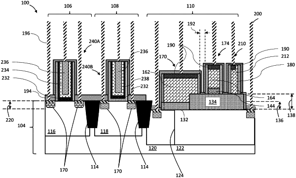
1. A transistor structure, comprising:
a doped well region within a substrate, the doped well region including a first doped well abutting a second doped well at a boundary, wherein the first doped well has an opposite doping type from the second doped well;
a dielectric layer, including:
a first portion over the first doped well, the second doped well, and the boundary and having a first height above the doped well region, and
a second portion immediately adjacent the first portion and over the second doped well, and having a second height above the doped well region greater than the first height;
a first gate structure on the first portion of the dielectric layer and over the boundary between the first doped well and the second doped well; and
a second gate structure on the second portion of the dielectric layer and over the second doped well,
wherein the second portion of the dielectric layer is under the first gate structure and the second gate structure.
|