| CPC H01L 21/26513 (2013.01) [H01L 21/3065 (2013.01); H01L 21/3212 (2013.01); H01L 21/76859 (2013.01); H01L 21/76877 (2013.01)] | 18 Claims |
|
1. A method of promoting adhesion between a dielectric layer of a semiconductor device and a metal fill deposited within a trench in the dielectric layer, the method comprising:
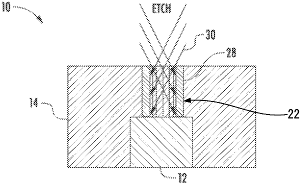
performing an ion implantation process wherein an ion beam formed of an ionized dopant species is directed into the trench at an acute angle relative to a top surface of the dielectric layer to form an implantation layer in a sidewall of the trench;
etching the implantation layer back to a depth where a concentration of the implanted dopant species is higher than in other portions of the implantation layer; and
depositing a metal fill in the trench atop an underlying bottom metal layer, wherein the metal fill adheres to the sidewall.
|