| CPC H01L 21/2256 (2013.01) [H01L 21/02164 (2013.01); H01L 21/2257 (2013.01)] | 16 Claims |
|
1. A method for forming at least one doped zone configured to form a source and/or a drain of a transistor, comprising:
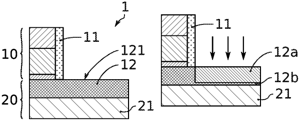
providing a stack comprising at least one active layer made from a semiconductor material formed directly on an insulating layer, and a transistor gate pattern located above the at least one active layer and having at least one lateral side extending in a plane substantially perpendicular to a face of the at least one active layer, the at least one lateral side being exposed, then
modifying a portion of the at least one active layer along an entire thickness of the at least one active layer so as to form a modified portion made of a modified semiconductor material, the modified portion extending in a region of the at least one active layer not overlaid by the gate pattern and extending down to the at least one lateral side of the gate pattern, the region of the at least one active layer located under the gate pattern forming a non-modified portion, then
forming a spacer on the at least one lateral side of the gate pattern,
removing the modified portion by selective etching of the modified semiconductor material with respect to the semiconductor material of the non-modified portion, so as to expose an edge of the non-modified portion, the edge extending substantially in an extension of the at least one lateral side of the gate pattern, and to expose the insulating layer, and
forming the doped zone by epitaxy starting from the exposed edge and extending over and in contact with the insulating layer.
|