| CPC H01L 21/0334 (2013.01) [G03F 7/70033 (2013.01); H01L 21/3083 (2013.01)] | 20 Claims |
|
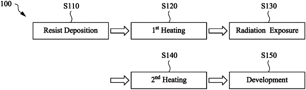
1. A method of manufacturing a semiconductor device, comprising:
forming a metallic photoresist layer, which is an alloy layer of two or more metal elements, over a target layer to be patterned;
selectively exposing the metallic photoresist layer to actinic radiation to form a latent pattern by changing a phase of an exposed portion of the alloy layer; and
developing the latent pattern by applying a developer to the selectively exposed photoresist layer to form a pattern,
wherein the metallic photoresist layer is deposited over the target layer by physical vapor deposition (PVD).
|