| CPC H01L 21/0217 (2013.01) [C23C 16/0272 (2013.01); C23C 16/345 (2013.01); C23C 16/45534 (2013.01); C23C 16/45536 (2013.01); H01L 21/02274 (2013.01); H01L 21/0228 (2013.01)] | 20 Claims |
|
1. A method of manufacturing a semiconductor structure, comprising:
providing a base; and
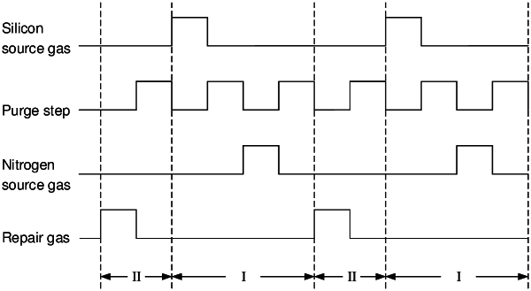
forming a silicon nitride film layer on the base by an atomic layer deposition process; wherein the atomic layer deposition process comprises multiple cyclic deposition steps; in each of the cyclic deposition steps, a silicon source gas and a nitrogen source gas are provided to a surface of the base;
wherein, before each of the cyclic deposition steps, the method of manufacturing a semiconductor structure further comprises a repair step; in the repair step, a repair gas is provided to the surface of the base, and the repair gas is a hydrogen-containing repair gas; the repair gas comprises a polar molecule for repairing the surface of the base that is damaged.
|