| CPC H01G 4/306 (2013.01) [H01G 4/012 (2013.01); H01G 4/33 (2013.01); H01G 4/008 (2013.01); H01G 4/1218 (2013.01); H01G 4/1227 (2013.01); H01G 4/1245 (2013.01); H01G 4/2325 (2013.01)] | 7 Claims |
|
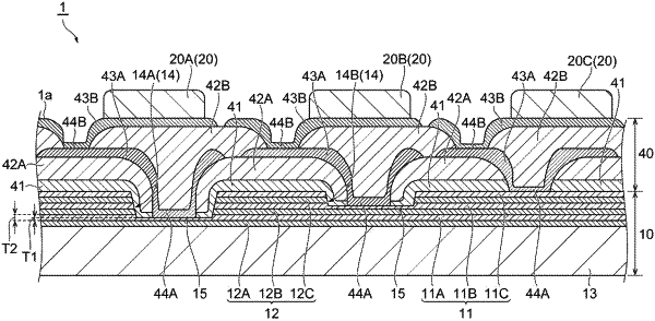
1. A thin film capacitor comprising a capacitance portion in which at least one dielectric layer is sandwiched between a pair of electrode layers included in a plurality of electrode layers,
wherein the capacitance portion has an opening which extends in a lamination direction in which the plurality of electrode layers and the dielectric layer are laminated and through which one electrode layer of the plurality of electrode layers is exposed,
the one electrode layer has an exposed portion exposed at a bottom surface of the opening,
the exposed portion is in contact with a wiring layer connecting the one electrode layer and an electrode terminal,
a thickness of the exposed portion of the one electrode layer is smaller than a thickness of other portions of the one electrode layer and is 50% or more of the thickness of the other portions of the one electrode layer,
the other portions of the one electrode layer are all portions other than the exposed portion, and
the wiring layer that is in contact with the exposed portion at the bottom surface of the opening is not in contact with another electrode layer in the opening.
|