| CPC H01G 4/30 (2013.01) [H01G 4/012 (2013.01); H01G 4/33 (2013.01); H01L 28/60 (2013.01); H01L 28/92 (2013.01)] | 6 Claims |
|
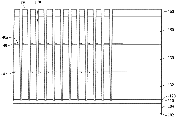
1. A method of manufacturing a semiconductor structure, comprising:
forming a first oxide layer over a landing pad layer;
forming a middle patterned dielectric layer over the first oxide layer, wherein the middle patterned dielectric layer comprises a plurality of openings exposing the first oxide layer;
forming a second oxide layer in the openings and over the middle patterned dielectric layer;
forming a top dielectric layer over the second oxide layer;
forming a trench through the top dielectric layer, the second oxide layer and the first oxide layer;
after forming the trench, conformally forming a bottom conductive layer on surfaces of the top dielectric layer, the second oxide layer, and the first oxide layer in the trench;
removing a portion of the top dielectric layer adjacent to the trench to expose a portion of the second oxide layer beneath the portion of the top dielectric layer; and
performing an etching process to remove the second oxide layer and the first oxide layer.
|