| CPC H01F 27/2804 (2013.01) [H01F 17/0013 (2013.01); H01F 27/29 (2013.01); H01F 41/043 (2013.01); H01F 41/10 (2013.01); H01F 41/122 (2013.01); H01F 2017/002 (2013.01); H01F 2017/004 (2013.01); H01F 2027/2809 (2013.01)] | 5 Claims |
|
1. An electronic component comprising:
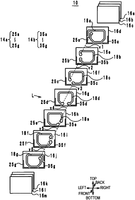
a multilayer body formed by laminating a plurality of insulation layers in a lamination direction, the multilayer body having a top surface, a bottom surface, a first end surface, and a second end surface each formed by outer edges of the insulation layers, the top surface opposite from the bottom surface, and the second end surface opposite from the first end surface;
an inductor, including a plurality of inductor conductor layers extending linearly and laminated with the insulation layers, the plurality of inductor conductor layers being connected by a plurality of via hole conductors that pass through ones of the insulation layers in the lamination direction, the inductor having a helical shape progressing from one side to another side in the lamination direction while winding;
a first outer electrode connected to the inductor and having an L-shape provided on the bottom surface and the first end surface; and
a second outer electrode connected to the inductor and having an L-shape provided on the bottom surface and the second end surface, wherein
the plurality of inductor conductor layers include a first inductor conductor layer directly connected to a part of the first outer electrode provided on the first end surface, and a second inductor conductor layer not directly connected to the first outer electrode and adjacent to the first inductor conductor layer on the other side in the lamination direction,
the plurality of via hole conductors including a first via hole conductor, connecting the first inductor conductor layer and the second inductor conductor layer, that is, when viewed in plan view from the lamination direction, provided closer to the first outer electrode than the second outer electrode,
a distance from the first via hole conductor to the top surface of the multilayer body is less than a distance from an uppermost surface of the first outer electrode to the top surface of the multilayer body, and
an end of the first inductor conductor layer having the first via hole conductor is extended in a direction toward the top surface of the multilayer body from the part of the first outer electrode.
|