| CPC H01F 27/2804 (2013.01) [H01F 17/0013 (2013.01); H01F 27/2828 (2013.01); H01F 27/29 (2013.01); H01F 2017/004 (2013.01); H01F 2017/0073 (2013.01); H01F 2027/2809 (2013.01)] | 20 Claims |
|
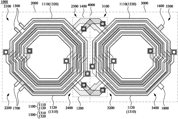
1. An inductor device, comprising:
a first inductor, comprising:
a first trace, located on a first layer; and
a second trace, located on a second layer, and coupled to the first trace in a first area and a second area respectively, wherein the first area and the second area are connected to each other at a junction;
a first connection member, disposed at a block at which the first trace and the second trace are not disposed and which is adjacent to the junction, and coupled to the second trace;
a second inductor, comprising:
a third trace, located on the first layer, wherein the first trace and the third trace are disposed in an interlaced manner in the first area and the second area respectively; and
a fourth trace, located on the second layer, and coupled to the third trace in the first area and the second area respectively, wherein the second trace and the fourth trace are disposed in an interlaced manner in the first area and the second area respectively; and
a second connection member, disposed at a block at which the third trace and the fourth trace are not disposed and which is adjacent to the junction, and coupled to the fourth trace.
|