| CPC G11C 7/222 (2013.01) [G06F 7/5443 (2013.01); G11C 7/1063 (2013.01); G11C 7/109 (2013.01); G11C 7/12 (2013.01); G11C 7/14 (2013.01); G11C 7/16 (2013.01)] | 20 Claims |
|
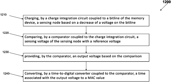
1. An Input/Output (I/O) circuit for a memory device, wherein the I/O circuit comprises:
a charge integration circuit coupled to a bitline of the memory device, wherein the charge integration circuit provides a sensing voltage based on a decrease of a voltage on the bitline;
a comparator coupled to the charge integration circuit, wherein the comparator compares the sensing voltage with a reference voltage and provides an output voltage based on the comparison; and
a time-to-digital converter coupled to the comparator, wherein the time-to-digital convertor converts a time associated with the output voltage to a digital value.
|