| CPC G11C 7/1096 (2013.01) [G11C 7/1051 (2013.01)] | 17 Claims |
|
14. A memory system, comprising:
one or more memory arrays; and
one or more controllers coupled with the one or more memory arrays and configured to cause the memory system to:
perform one or more first write operations on the one or more memory arrays according to a first pulse magnitude and a first pulse duration;
identify that a quantity of access operations performed on the one or more memory arrays satisfies a threshold; and
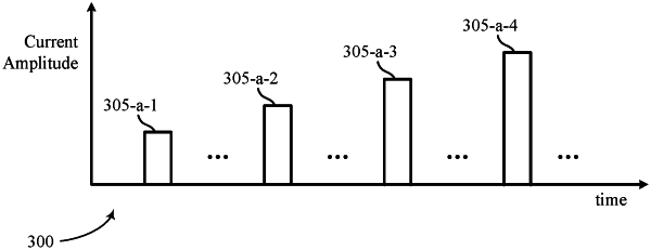
perform, based at least in part on identifying that the quantity of access operations performed on the one or more memory arrays satisfies the threshold, one or more second write operations on the one or more memory arrays according to a second pulse magnitude and a second pulse duration, wherein the second pulse magnitude is greater than the first pulse magnitude, and the second pulse duration is shorter than the first pulse duration.
|