| CPC G11C 7/1072 (2013.01) [G11C 5/06 (2013.01); G11C 7/1048 (2013.01); G11C 7/106 (2013.01); G11C 7/1087 (2013.01)] | 11 Claims |
|
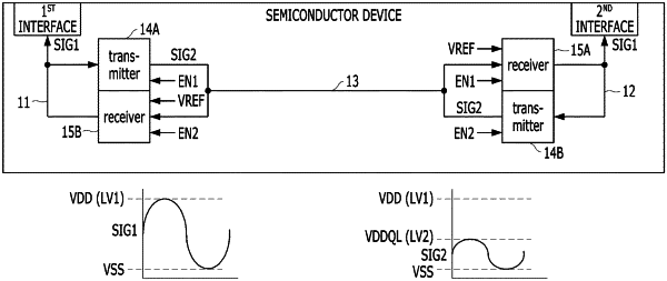
1. A semiconductor device comprising:
a first transmission path connected to a first interface and configured to transmit a first signal which swings between a ground level and a first voltage level;
a second transmission path connected to a second interface and configured to transmit the first signal;
a third transmission path configured to transmit a second signal which swings between the ground level and a second voltage level lower than the first voltage level;
a transmitter configured to:
receive the first signal through the first or second transmission path,
output the received first signal as the second signal to the third transmission path by changing the received first signal to have the level of the second signal, and
initialize an output terminal thereof in response to an enable signal; and
a receiver configured to:
receive the second signal through the third transmission path,
output the received second signal as the first signal through the first or second transmission path by changing the received second signal to have the level of the first signal,
determine a logic level of the second signal, which is applied to an input terminal thereof, through a reference voltage level that is regulated according to a fed-back logic level of an output terminal thereof, and
initialize the output terminal thereof in response to the enable signal.
|