| CPC G11C 7/1063 (2013.01) [G11C 7/1039 (2013.01); G11C 7/109 (2013.01); G11C 8/06 (2013.01)] | 17 Claims |
|
1. A memory system comprising:
a plurality of semiconductor memory devices; and
a control device, wherein
each of the semiconductor memory devices includes:
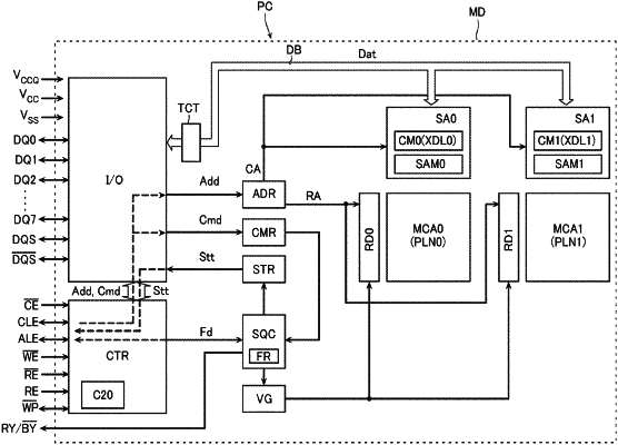
a first pad to which a first signal is input;
a second pad to which a second signal is input;
a third pad to which a third signal is input;
a memory cell array including a string in which a plurality of memory cell transistors are connected in series;
a sense amplifier connected to the memory cell array;
a data register that is connected to the sense amplifier and is capable of storing data read out from the memory cell array;
a control circuit being capable of executing a data out operation that outputs the data stored in the data register from the second pad, wherein
in a first mode, after the first signal input to the first pad is switched, each of the semiconductor memory devices retrieves a command set instructing the data out operation, via the second pad, and,
in a second mode, after the first signal input to the first pad is switched, each of the semiconductor memory devices retrieves the command set instructing the data out operation, via at least the third pad, and
the control device executes a first operation assigning different addresses to the respective semiconductor memory devices and a second operation causing the modes of the respective semiconductor memory devices to be switched from the first mode to the second mode.
|