| CPC G11C 7/065 (2013.01) [G11C 7/08 (2013.01)] | 20 Claims |
|
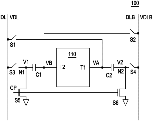
1. A circuit comprising:
a reference voltage node;
first and second data lines;
a sense amplifier comprising first and second input terminals;
a first switching device coupled between the first data line and the first input terminal;
a second switching device coupled between the second data line and the second input terminal;
a third switching device coupled between the first data line and a first node;
a fourth switching device coupled between the second data line and a second node;
a fifth switching device coupled between the first node and the reference voltage node;
a sixth switching device coupled between the second node and the reference voltage node;
a first capacitive device coupled between the first node and the second input terminal; and
a second capacitive device coupled between the second node and the first input terminal,
wherein the circuit is configured to
in a first operational mode, switch on each of the first through fourth switching devices and switch off each of the fifth and sixth switching devices, and
in a second operational mode, switch off each of the first through fourth switching devices and switch on each of the fifth and sixth switching devices.
|