| CPC G11C 29/42 (2013.01) [G11C 29/18 (2013.01); G11C 29/36 (2013.01); G11C 29/785 (2013.01); G11C 2029/1802 (2013.01)] | 10 Claims |
|
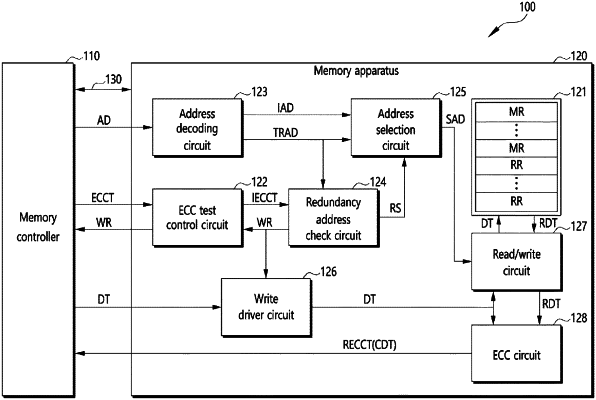
1. A memory apparatus comprising:
an address decoding circuit configured to output a test redundancy address based on an address that is transmitted from a memory controller; and
a redundancy address check circuit configured to determine whether the test redundancy address is replacing a failed address by comparing the test redundancy address with a reference address, in an ECC test operation,
wherein the reference address is a redundancy address that was most recently used to replace a failed address.
|