| CPC G11C 29/14 (2013.01) [G11C 29/08 (2013.01); G11C 29/18 (2013.01); G11C 2029/1802 (2013.01)] | 20 Claims |
|
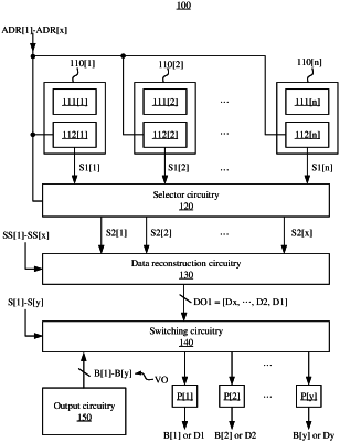
1. A chip having debug function, comprising:
a plurality of functional circuitries configured to respectively generate a plurality of sets of debug signals, wherein each of the plurality of functional circuitries comprises a decoder circuit configured to store a corresponding set of debug signals in the plurality of sets of debug signals and output a corresponding debug signal in the corresponding set of debug signals to be a corresponding signal in a plurality of first signals according to a corresponding address signal in a plurality of address signals;
a selector circuitry configured to select a plurality of second signals from the plurality of first signals according to the plurality of address signals;
a data reconstruction circuitry configured to select a plurality of first data from the plurality of second signals according to a plurality of split signals and output the plurality of first data to be first debug data, wherein each of the plurality of first data is partial data of a corresponding signal in the plurality of second signals; and
a switching circuitry configured to determine whether to output the first debug data or at least one output signal associated with the plurality of functional circuitries via a plurality of output ports according to a plurality of switching signals.
|