| CPC G11C 19/28 (2013.01) [G09G 3/3677 (2013.01); G09G 3/3696 (2013.01); G11C 19/184 (2013.01); H01L 25/03 (2013.01); H01L 27/1222 (2013.01); H01L 27/1225 (2013.01); H01L 27/124 (2013.01); H01L 27/1251 (2013.01); H01L 27/127 (2013.01); H01L 27/1288 (2013.01); H03K 19/0013 (2013.01); H05K 7/02 (2013.01); G09G 2300/0809 (2013.01); G09G 2310/0286 (2013.01); H01L 2924/0002 (2013.01)] | 2 Claims |
|
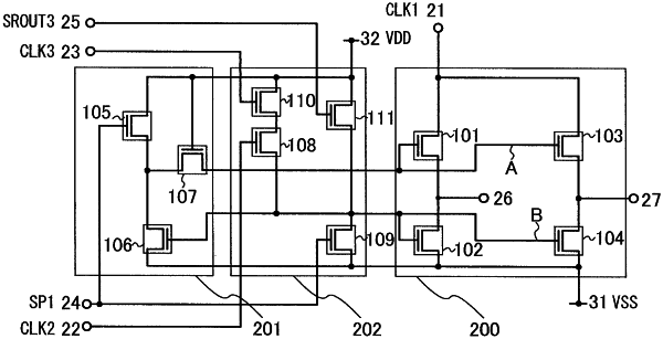
1. A semiconductor device comprising:
a first transistor, a second transistor, a third transistor, a fourth transistor, a fifth transistor, a sixth transistor and a seventh transistor,
wherein each of the first transistor, the second transistor, the third transistor, the fourth transistor, the fifth transistor, the sixth transistor and the seventh transistor includes an oxide semiconductor layer in a channel region,
wherein a first clock signal is configured to be input to one of a source and a drain of the first transistor,
wherein the other of the source and the drain of the first transistor is directly connected to an output terminal,
wherein one of a source and a drain of the second transistor is directly connected to a power supply line,
wherein the other of the source and the drain of the second transistor is directly connected to the output terminal,
wherein one of a source and a drain of the third transistor is electrically connected to a gate of the first transistor,
wherein a start pulse is configured to be input to a gate of the third transistor,
wherein one of a source and a drain of the fourth transistor is electrically connected to the power supply line,
wherein the other of the source and the drain of the fourth transistor is electrically connected to the gate of the first transistor,
wherein one of a source and a drain of the fifth transistor is directly connected to a gate of the fourth transistor,
wherein one of a source and a drain of the sixth transistor is directly connected to the gate of the fourth transistor,
wherein one of a source and a drain of the seventh transistor is electrically connected to the gate of the fourth transistor,
wherein the other of the source and the drain of the seventh transistor is electrically connected to the power supply line,
wherein a second clock signal is configured to be input to a gate of the fifth transistor,
wherein a clock signal is not input to a gate of the sixth transistor,
wherein a ratio of a channel width to a channel length of the third transistor is larger than a ratio of a channel width to a channel length of the fourth transistor, and
wherein a channel width of the fifth transistor is smaller than a channel width of the sixth transistor.
|