| CPC G11C 17/18 (2013.01) [G11C 7/18 (2013.01); H10B 20/00 (2023.02)] | 20 Claims |
|
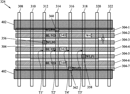
1. A semiconductor device, comprising:
a first conductive via that electrically couples a first metal line to a first gate structure in a first active region, wherein the first conductive via is disposed over the first active region; and
a second metal line parallel to the first metal line and electrically coupled to a source/drain region of the first active region by a second conductive via;
wherein the first and second metal lines are formed within a same interconnect layer; and
wherein the first active region is associated with a first memory cell including a first program word line, a second program word line, a first read word line, and a second read word line.
|