| CPC G11C 16/3459 (2013.01) [G11C 11/5628 (2013.01); G11C 11/5671 (2013.01); G11C 16/0483 (2013.01); G11C 16/10 (2013.01)] | 20 Claims |
|
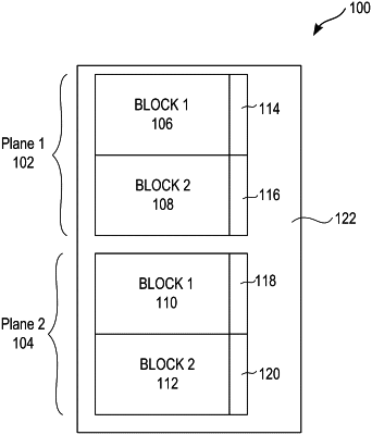
1. A memory device, comprising:
memory cells; and
a first latch circuit, a second latch circuit, and a third latch circuit, coupled to the memory cells,
wherein the first latch circuit is configured to store verification data during a verification operation,
the second latch circuit is configured to store failure pattern data during the verification operation,
the third latch circuit is configured to store program data,
the verification data comprises inhibit information and inverted inhibit information, and
the inverted inhibit information is configured to indicate unverified states of the memory cells that include a first state and remaining states subsequent to the first state.
|