| CPC G11C 16/30 (2013.01) [G11C 16/0483 (2013.01); G11C 16/08 (2013.01); G11C 16/24 (2013.01); G11C 11/5621 (2013.01); G11C 11/5671 (2013.01)] | 17 Claims |

|
1. A system comprising:
a compensation circuit configured to:
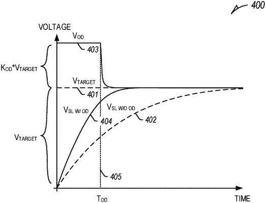
provide a number of different bias signals to each of multiple signal lines of an array of memory cells, each signal line configured to provide access to a group of memory cells of the array of memory cells, each bias signal having an overdrive voltage above a target voltage by a selected increment and an overdrive period;
determine settling times of each of the multiple signal lines to the target voltage for the number of different bias signals;
determine a functional compensation profile for the array of memory cells comprising a relationship between the different bias signals and the determined settling times across the multiple signal lines in a number of separate linear segments greater than one but less than N/2, wherein N is the number of multiple signal lines; and
store a representation of the determined functional compensation profile to compensate for variance in an electrical parameter across the signal lines of the array of memory cells.
|