| CPC G11C 16/28 (2013.01) [G06N 3/063 (2013.01); G11C 11/54 (2013.01); G11C 16/0466 (2013.01); G11C 16/10 (2013.01); G11C 16/16 (2013.01); H01L 29/4234 (2013.01); H01L 29/792 (2013.01)] | 6 Claims |
|
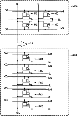
1. A semiconductor device comprising:
a plurality of nonvolatile memory cells;
a plurality of reference-current cells; and
a sense amplifier electrically connected to the plurality of nonvolatile memory cells and the plurality of reference-current cells and comparing an electric current flowing in each of the plurality of nonvolatile memory cells and an electric current flowing in each of the plurality of reference-current cells,
wherein each of the plurality of nonvolatile memory cells and the plurality of reference-current cells includes:
a first gate dielectric film formed on a semiconductor substrate;
a second gate dielectric film formed on the semiconductor substrate and having a charge accumulating layer;
a first gate electrode formed on the first gate dielectric film;
a second gate electrode formed on the second gate dielectric film;
a drain region formed in a region of the semiconductor substrate close to the first gate electrode; and
a source region formed in a region of the semiconductor substrate close to the second gate electrode,
wherein a writing operation or an erasing operation is performed to each of the plurality of reference-current cells when the writing operation or the erasing operation is performed to each of the plurality of nonvolatile memory cells,
wherein the first gate electrode and the second gate electrode of each of the plurality of nonvolatile memory cells and the plurality of reference-current cells extend in a first direction in a plan view, and are adjacent to each other in a second direction crossing the first direction in a plan view, and
wherein a width of the semiconductor substrate in the first direction under each of the first gate electrode and the second gate electrode of the plurality of reference-current cells is larger than a width of the semiconductor substrate in the first direction under each of the first gate electrode and the second gate electrode of the plurality of nonvolatile memory cells.
|