| CPC G11C 16/24 (2013.01) [G11C 16/0483 (2013.01); G11C 16/08 (2013.01); G11C 29/12005 (2013.01)] | 20 Claims |

|
1. A memory device comprising:
a memory cell block connected between a common source line and a bit line and including a plurality of NAND strings, wherein the plurality of NAND strings includes a string selection transistor, a plurality of memory cells, and a ground selection transistor;
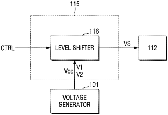
a voltage generating circuit generating a high voltage signal, a shielding signal, and a logic signal for the memory cell block;
a row decoder connected to the memory cell block through a word line;
a page buffer connected to the memory cell block through the bit line;
a peripheral circuit including a shielding signal switching circuit and a control logic circuit controlling the voltage generating circuit, the row decoder, and the page buffer;
a first wiring providing the high voltage signal to the memory cell block;
a second wiring providing the logic signal to the memory cell block; and
a third wiring providing the shielding signal to the memory cell block,
wherein the shielding signal switching circuit applies the shielding signal to the third wiring at a first voltage level in a first mode, and applies the shielding signal to the third wiring at a second voltage level different from the first voltage level in a second mode.
|