US 11,942,160 B2
Performing a program operation based on a high voltage pulse to securely erase data
Kishore Kumar Muchherla, San Jose, CA (US); Harish R. Singidi, Fremont, CA (US); Vamsi Pavan Rayaprolu, Santa Clara, CA (US); Ashutosh Malshe, Fremont, CA (US); and Sampath K. Ratnam, San Jose, CA (US)
Assigned to Micron Technology, Inc., Boise, ID (US)
Filed by Micron Technology, Inc., Boise, ID (US)
Filed on Dec. 12, 2022, as Appl. No. 18/079,843.
Application 18/079,843 is a continuation of application No. 17/062,453, filed on Oct. 2, 2020, granted, now 11,527,291.
Claims priority of provisional application 62/977,126, filed on Feb. 14, 2020.
Prior Publication US 2023/0110545 A1, Apr. 13, 2023
This patent is subject to a terminal disclaimer.
Int. Cl. G11C 16/14 (2006.01); G11C 16/08 (2006.01); G11C 16/26 (2006.01); G11C 16/30 (2006.01); G11C 16/34 (2006.01)
CPC G11C 16/14 (2013.01) [G11C 16/08 (2013.01); G11C 16/26 (2013.01); G11C 16/30 (2013.01); G11C 16/3404 (2013.01)] 17 Claims
OG exemplary drawing
 
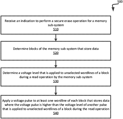
1. A method comprising:
receiving a request to perform a secure erase operation for a memory component;
determining a voltage level of a pass voltage applied to unselected wordlines of the memory component during a read operation; and
applying, by a processing device, a voltage pulse during a program operation to at least one wordline of the memory component to perform the secure erase operation, the voltage pulse exceeding the pass voltage applied to the unselected wordlines of the memory component during the read operation, wherein each memory cell of the at least one wordline is in an open state in response to an application of the voltage pulse to the at least one wordline during a subsequent read operation.