| CPC G11C 16/10 (2013.01) [G11C 16/08 (2013.01); G11C 16/26 (2013.01); G11C 16/3459 (2013.01); G11C 7/06 (2013.01)] | 20 Claims |
|
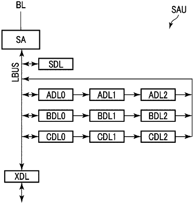
1. A memory device including:
a memory string;
a sense amplifier connected to the memory string through a bit line;
a signal line connected to the sense amplifier;
a first latch including a first input and a first output, the first input of the first latch connected to the signal line;
a second latch including a second input and a second output, the second input of the second latch connected to the first output of the first latch; and
a third latch including a third input and a third output, the third input of the third latch connected to the second output of the second latch, the third output of the third latch connected to the signal line.
|