| CPC G11C 16/0433 (2013.01) [G11C 5/063 (2013.01); G11C 16/08 (2013.01); G11C 16/20 (2013.01)] | 20 Claims |
|
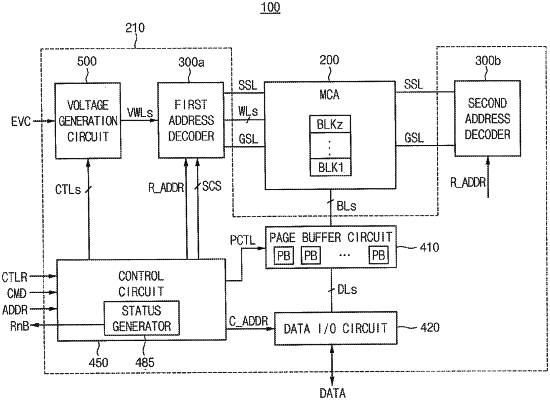
1. A nonvolatile memory device, comprising:
a first semiconductor layer comprising:
an upper substrate in which a plurality of word-lines extending in a first horizontal direction, at least one string selection line, at least one ground selection line, and a plurality of bit-lines extending in a second horizontal direction substantially perpendicular to the first horizontal direction are disposed; and
a memory cell array including at least one memory block disposed on the upper substrate; and
a second semiconductor layer disposed under the first semiconductor layer in a vertical direction substantially perpendicular to the first and second horizontal directions, wherein the second semiconductor layer includes a first address decoder and a second address decoder,
wherein the at least one memory block includes a cell region including a plurality of memory cells, a first extension region disposed in a first side of the cell region, and a second extension region disposed in a second side of the cell region, the second side opposed to the first side,
wherein the first address decoder is disposed under the first extension region and includes a plurality of first pass transistors configured to drive the plurality of word-lines, the at least one string selection line and the at least one ground selection line, and
wherein the second address decoder is disposed under the second extension region and includes a plurality of second pass transistors configured to drive the at least one string selection line and the at least one ground selection line.
|