| CPC G11C 16/0433 (2013.01) [G11C 7/06 (2013.01); G11C 16/08 (2013.01); G11C 16/24 (2013.01); G11C 16/26 (2013.01); G11C 16/30 (2013.01)] | 20 Claims |
|
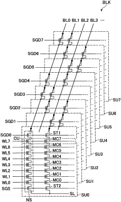
1. A semiconductor memory device comprising:
a first string unit including a first memory string including a first selection transistor and a first memory cell coupled to the first selection transistor;
a second string unit including a second memory string including a second selection transistor and a second memory cell coupled to the second selection transistor;
a first select gate line that is coupled to the first selection transistor;
a second select gate line that is coupled to the second selection transistor and is different from the first select gate line;
a first bit line that is coupled to the first string unit and is not coupled to the second string unit;
a second bit line that is coupled to the second string unit and is not coupled to the first string unit; and
a first word line that is coupled to the first memory cell and the second memory cell,
wherein both of the first select gate line and the second select gate line are selected in a first read operation, and
the first select gate line is selected and the second select gate line is not selected in a second read operation.
|