US 11,942,150 B2
RRAM circuit
Chung-Cheng Chou, Hsinchu (TW); Zheng-Jun Lin, Hsinchu (TW); and Pei-Ling Tseng, Hsinchu (TW)
Assigned to TAIWAN SEMICONDUCTOR MANUFACTURING COMPANY, LTD., Hsinchu (TW)
Filed by TAIWAN SEMICONDUCTOR MANUFACTURING COMPANY, LTD., Hsinchu (TW)
Filed on Nov. 10, 2022, as Appl. No. 18/054,359.
Application 17/200,416 is a division of application No. 16/415,785, filed on May 17, 2019, granted, now 10,950,303, issued on Mar. 16, 2021.
Application 18/054,359 is a continuation of application No. 17/200,416, filed on Mar. 12, 2021, granted, now 11,527,285.
Claims priority of provisional application 62/679,557, filed on Jun. 1, 2018.
Prior Publication US 2023/0072287 A1, Mar. 9, 2023
This patent is subject to a terminal disclaimer.
Int. Cl. G11C 11/00 (2006.01); G11C 13/00 (2006.01)
CPC G11C 13/0038 (2013.01) [G11C 13/003 (2013.01); G11C 2213/15 (2013.01); G11C 2213/79 (2013.01)] 20 Claims
OG exemplary drawing
 
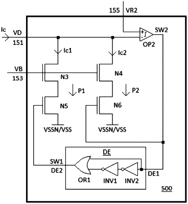
1. A resistive random-access memory (RRAM) circuit comprising:
an RRAM device configured to output a cell current responsive to a bit line voltage; and
a current limiter comprising:
an input terminal coupled to the RRAM device;
first and second parallel current paths configured to conduct the cell current between the input terminal and a reference voltage node; and
an amplifier configured to generate a first signal responsive to a voltage level at the input terminal and a reference voltage level,
wherein each of the first and second current paths comprises a switching device configured to selectively conduct a portion of the cell current responsive to the first signal.