| CPC G11C 13/0007 (2013.01) [G11C 13/0069 (2013.01); H10B 63/34 (2023.02); H10B 63/80 (2023.02); H10N 70/011 (2023.02); H10N 70/253 (2023.02); H10N 70/841 (2023.02); H10N 70/8833 (2023.02)] | 20 Claims |
|
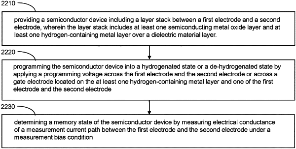
1. A method of operating a semiconductor device, comprising:
providing a semiconductor device including a layer stack between a first electrode and a second electrode, wherein the layer stack includes at least one semiconducting metal oxide layer and at least one hydrogen-containing metal layer over a dielectric material layer;
programming the semiconductor device into a hydrogenated state or a de-hydrogenated state by applying a programming pulse across the first electrode and the second electrode or across a gate electrode located on the at least one hydrogen-containing metal layer and one of the first electrode and the second electrode, wherein the hydrogenated state is a state in which the at least one semiconducting metal oxide layer is impregnated with hydrogen atoms and wherein the de-hydrogenated state is a state in which the at least one semiconducting metal oxide layer is hydrogen-depleted; and
determining a memory state of the semiconductor device.
|